|
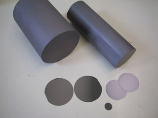
SICO product range includes wafers from 4" to 8" diameter in usual orientations.
The wafers are produced with resistance and doping are requested by the customer.
SICO quality control system assures adherence to the SEMI-Standards
SICO wafer manufacture in SICO Jena Germany Factory. We accept small & large quantity order in fast delivery with competitive price. 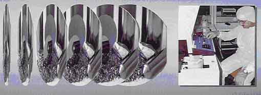
Wafer Processing
The ingot is characterized by various measurements (electrical resistance, conduction type, orientation)As the next step the ingot is ground cylindrically, then flatted and sliced.Afterwards the wafer is lapped to remove the saw marks. Good wafer geometry is largely determined by the lapping process. The edges are rounded in order to avoid chipping during the subsequent polishing process.Surface damage from lapping is then reworked by etching.The wafer is polished in two steps
- Stock removal
- Fine polishing
Final control and cleaning is done by latest technology method. |

 SILICON WAFER